


-
Large superconducting magnet[1-3] is commonly used in magnetic confinement fusion devices to provide strong magnetic field for confining the plasma. The quench accident, which means the superconductor suddenly changes from zero resistance state to normal state resistance state, can cause a rapid temperature rise with high Joule heat and even burn the magnet[4-8]. Therefore, the quench protection system (QPS)[9-12] is essential for the safe operation of superconductors.
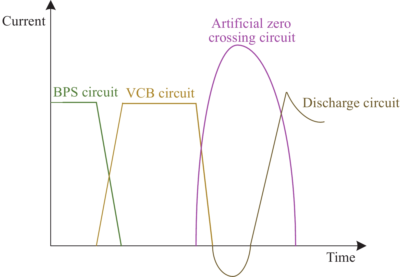
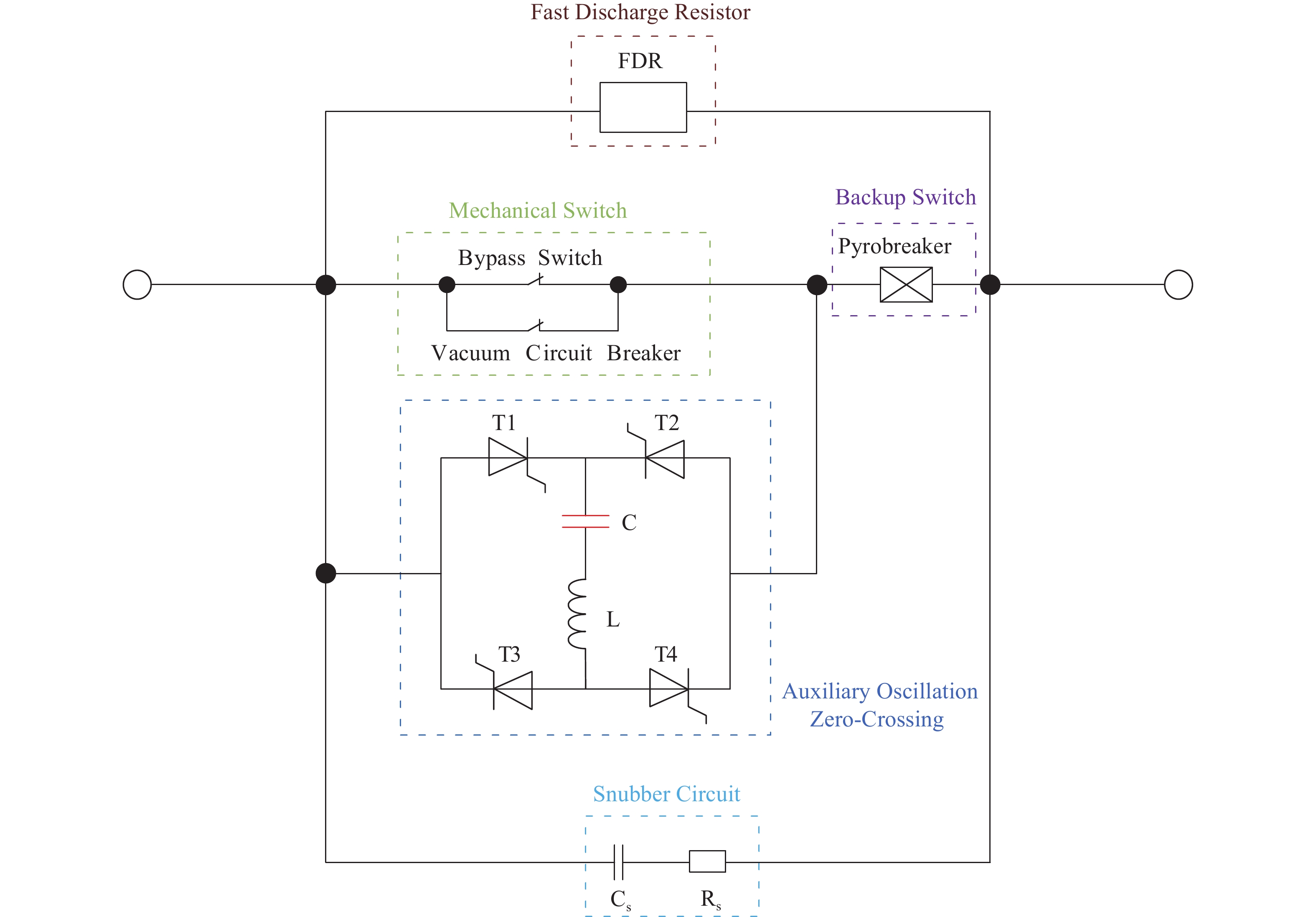
The topology of QPS in the comprehensive research facility for fusion technology (CRAFT) is shown in Fig. 1, where the auxiliary oscillation zero-crossing circuit consists of the charging capacitor, pulse inductor and four thyristor stacks. The bypass switch carries a steady state of 100 kA current, the vacuum circuit breaker (VCB) can interrupt the high current with the auxiliary oscillation zero-crossing circuit, and the fast discharge resistor is used to consume energy stored in the magnet. The control logic and current transfer diagram of QPS[13-15] are shown in Fig. 2.
Figure 1. Topology of QPS in CRAFT
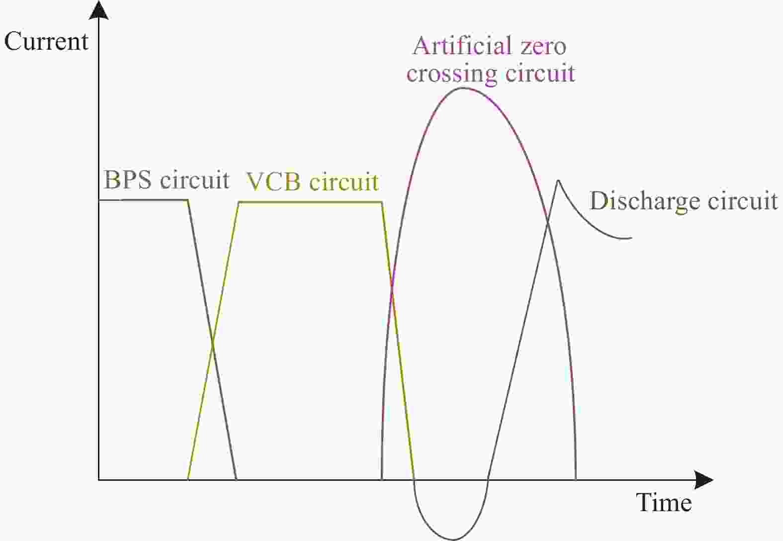
Figure 2. Control logic and current transfer waveform of QPS
However, under high current conditions, the pulse inductor generates a magnetic field, which subjects the connecting devices within the auxiliary oscillation circuit of QPS to electromagnetic forces, leading to deformation. Consequently, the reliability of the QPS is significantly reduced. Therefore, it is necessary to analyze and optimize the magnetic field of pulse inductor.
In this paper, the working process and importance of pulsed inductors in the auxiliary oscillation zero-crossing circuit are introduced in detail. The magnetic induction intensity of the pulse inductor at any point in space can be calculated by using an equivalent mathematical model based on the physical model, and simulations can be used to determine the distribution of the magnetic field around the pulse inductor and how it affects the nearby equipment. The ideal selection of shielding plate material and shape is covered in this paper along with an electromagnetic shielding method that is suggested. The findings have broad repercussions for upcoming reliability research on auxiliary oscillation zero-crossing systems[16-18].
-
In the QPS, the commutation circuit generates a high amplitude pulse current by using the charging capacitor to oscillate with a pulse inductor. The pulse current flows in reverse through the main circuit vacuum switch, creating an artificial zero-crossing point for it to shut down. A simplified diagram of the current transfer process is shown in Fig. 3.
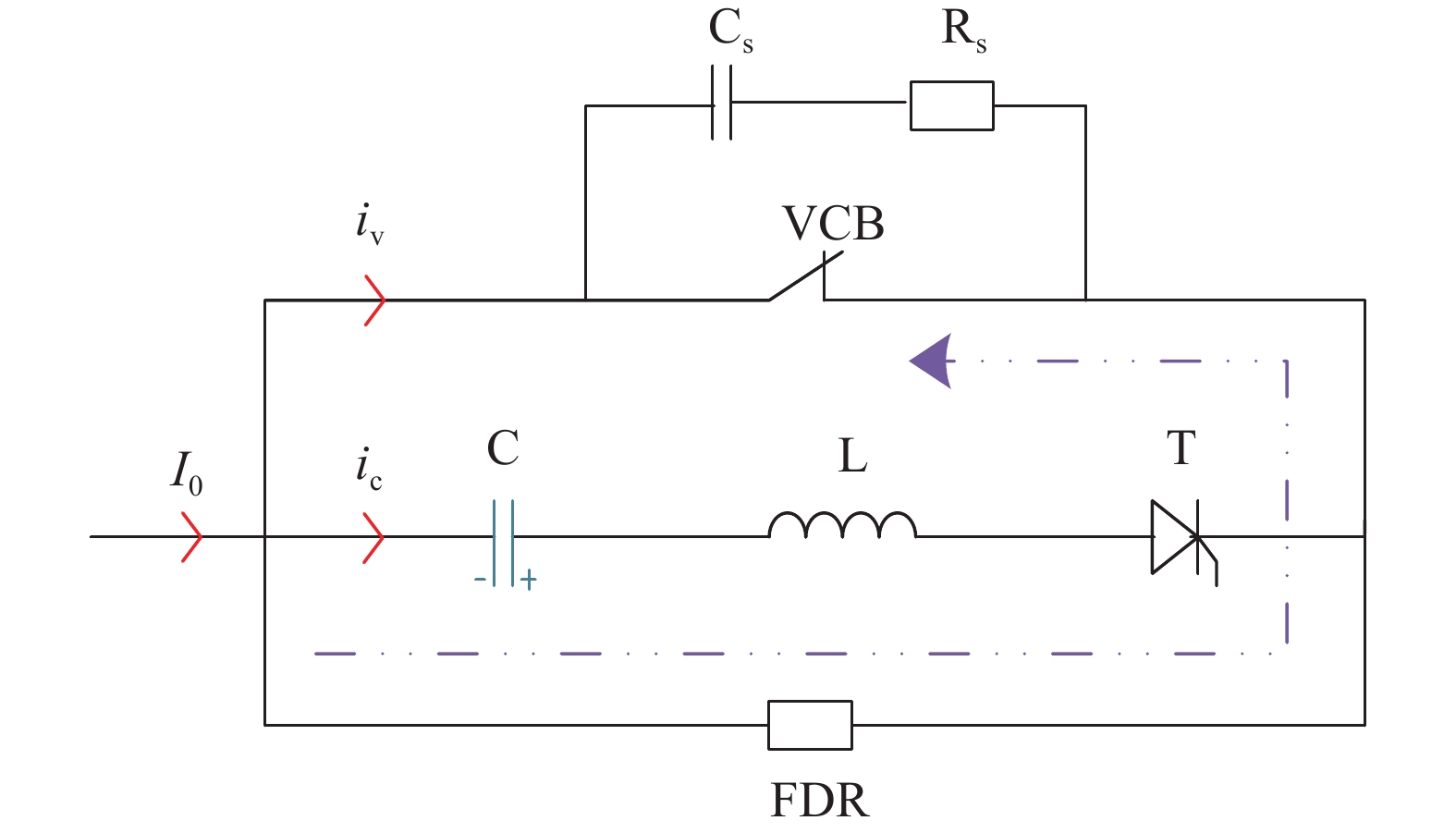
Figure 3. Simplified diagram of current transfer process
In Fig. 3, the thyristor T control is turned on, and the charging capacitor and pulse inductor release the reverse pulse current to the vacuum switching branch, thus forcing the current down to achieve zero-crossing shutdown. Assuming that the thyristor is turned on at t0, the VCB current decreases to zero at t1. The analytical equations of the circuit in this process are obtained as follows:
$$ {I}_{0}={i}_{{\mathrm{V}}}+{i}_{{\mathrm{C}}} $$ (1) $$ {u}_{{\mathrm{c}}}={U}_{{\mathrm{co}}}-\dfrac{1}{C}\int {i}_{{\mathrm{C}}}{\mathrm{d}}t $$ (2) $$ i_{\mathrm{C}}=C\dfrac{\mathrm{d\mathit{u}}_{\mathrm{c}}}{\mathrm{d}t} $$ (3) In the above equation:
$ {I}_{0} $ —— magnet current (A);
$ {i}_{{\mathrm{V}}} $ —— VCB current (A);
$ {i}_{{\mathrm{C}}} $ —— artificial zero-crossing loop current (A);
$ {U}_{{\mathrm{co}}} $ —— charging capacitor voltage (V);
$ {u}_{{\mathrm{c}}} $ —— capacitor voltage (V).
After derivation, the following equations are obtained.
$$ i_{\mathrm{V}}=I_0-U_{\mathrm{co}}\sqrt{\dfrac{C}{L}}\mathrm{sin}\left[\sqrt{\dfrac{1}{LC}}\left(t-t_0\right)\right] $$ (4) $$ i_{\mathrm{V}}=I_0-U_{\mathrm{co}}\sqrt{\dfrac{C}{L}}\mathrm{sin\left[\sqrt{\dfrac{1}{\mathit{LC}}}\left(\mathit{t}-\mathit{t}_0\right)\right]} $$ (5) $$ u_{\mathrm{c}}=U_{\mathrm{co}}\mathrm{cos}\left[\sqrt{\dfrac{1}{LC}}\left(t-t_0\right)\right] $$ (6) The pulse inductor in the converter communication circuit plays the role of regulating the pulse current width and controlling the pulse current amplitude and rate of change, and plays a vital role in whether the vacuum switch can be turned off reliably. Therefore, communication circuit parameters need to be calculated.
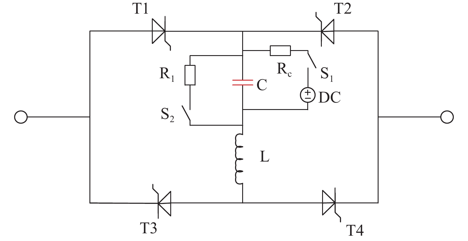
As shown in Fig. 4, the auxiliary oscillation zero-crossing circuit consists of charging capacitor C, pulse inductor L and thyristor bridges (T1, T2, T3, T4), which can realize bidirectional fault current opening and closing, S1 is the charging circuit control switch of charging capacitor, Rc is the charging current limiting resistor; S2 is the discharging circuit control switch, R1 is the discharging resistor of charging capacitor.

Figure 4. Topology of auxiliary oscillation zero-crossing circuit for QPS
Based on the technical parameters in Tab. 1, the oscillation discharge loop parameters were determined. For the magnet supply voltage level, the preset voltage of the commutation circuit $ {U}_{{\mathrm{co}}} $ is 12 kV, and the initial rise rate of the commutation pulse current is controlled below 190 A/μs, ignoring the influence of the thyristor bridge arm parameters on the commutation process.
Technical parameters Value $ \left|{\mathrm{d}}i/{\mathrm{d}}t\right| $max/(A·μs−1) 100~200 $ \left|{\mathrm{d}}u/{\mathrm{d}}t\right| $max/(V·μs−1) 200~500 tcom/μs $ \geqslant 300 $ $ {U}_{{\mathrm{co}}} $/kV 5~12 Table 1. Technical parameters of commutation circuit
$$ \dfrac{{U}_{{\mathrm{c}}}}{L}\leqslant 190\;\mathrm{A}/\mathrm{\mu }\mathrm{s} $$ (7) The calculation shows that $ L\geqslant 63.2$ μH, the actual use of 66 μH.
Considering the current margin, taking the safety circulating current factor $ k $ = 1.2, the peak commutation $ {I}_{{\mathrm{P}}} $ current is shown as Eq. (8):
$$ {I}_{{\mathrm{P}}}={U}_{{\mathrm{c}}}\sqrt{\dfrac{C}{L}}=k{I}_{{\mathrm{m}}}=1.2\times 100\;\mathrm{k}\mathrm{A}=120\;\mathrm{k}\mathrm{A} $$ (8) -
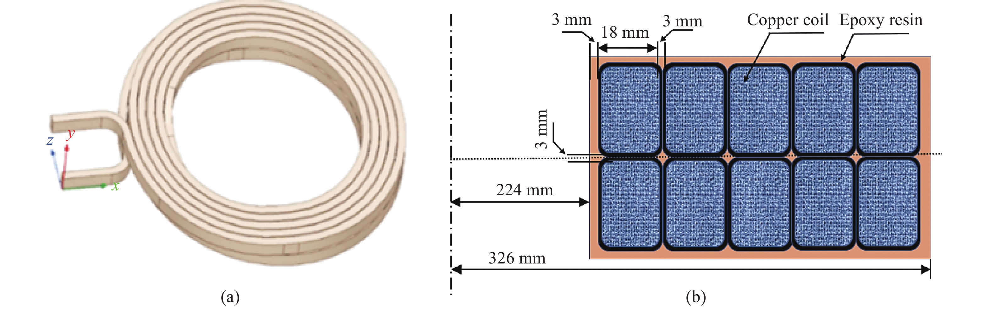
Copper conductor[19] is chosen as the inductor material based on the pulse inductor's operating circumstances, the needed stray parameters, cost performance requirements, and space requirements. The circular design of the inductor coils, as seen in Fig. 5, effectively avoids the challenges presented by square solenoids and lessens the skin effect. The inductor's coils are roughly concentrically arranged, which can equally distribute magnetic stress on the coils and lessen electromagnetic force damage to the coil structure.

Figure 5. Model diagram of pulse inductor
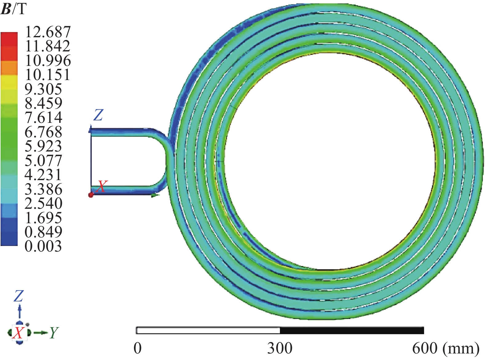
According to the model and relevant calculation parameters in Fig. 6 and Tab. 2, the simulation of the pulsed inductor operating at 120 kA operating condition is carried out in ANSYS, and the internal magnetic force line vector diagram and magnetic field cloud diagram of the coil are obtained. The simulation results are shown in Fig. 7 and Fig. 8.
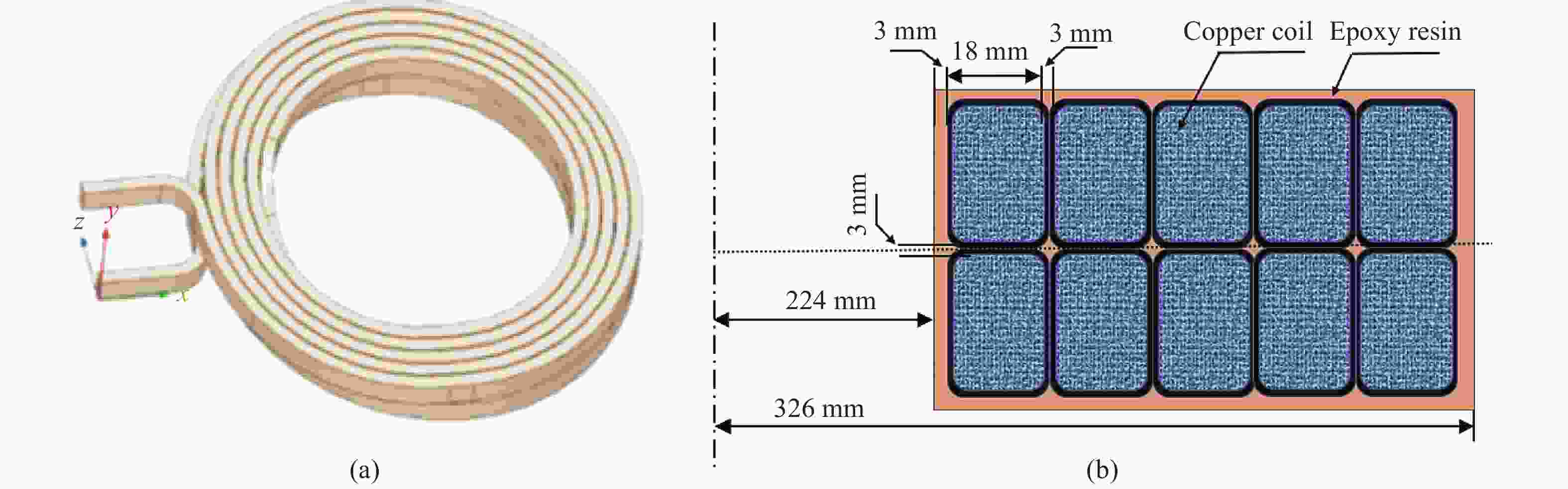
Figure 6. 3D model of pulse inductor coil
Parameters Values Conductor dimension/mm$ \times $mm 25$ \times $18 Inside diameter/mm 448 Outside diameter/mm 652 Height/mm 53 Turn number/turn 5 Layer number/turn 2 Excitation current/kA 120 Current frequency/Hz 400 Table 2. 3D finite element simulation to calculate the relevant parameters
As can be seen from Fig. 7 and Fig. 8, the pulse inductor's maximum magnetic induction intensity is 12.7 T for a 120 kA pulse current.
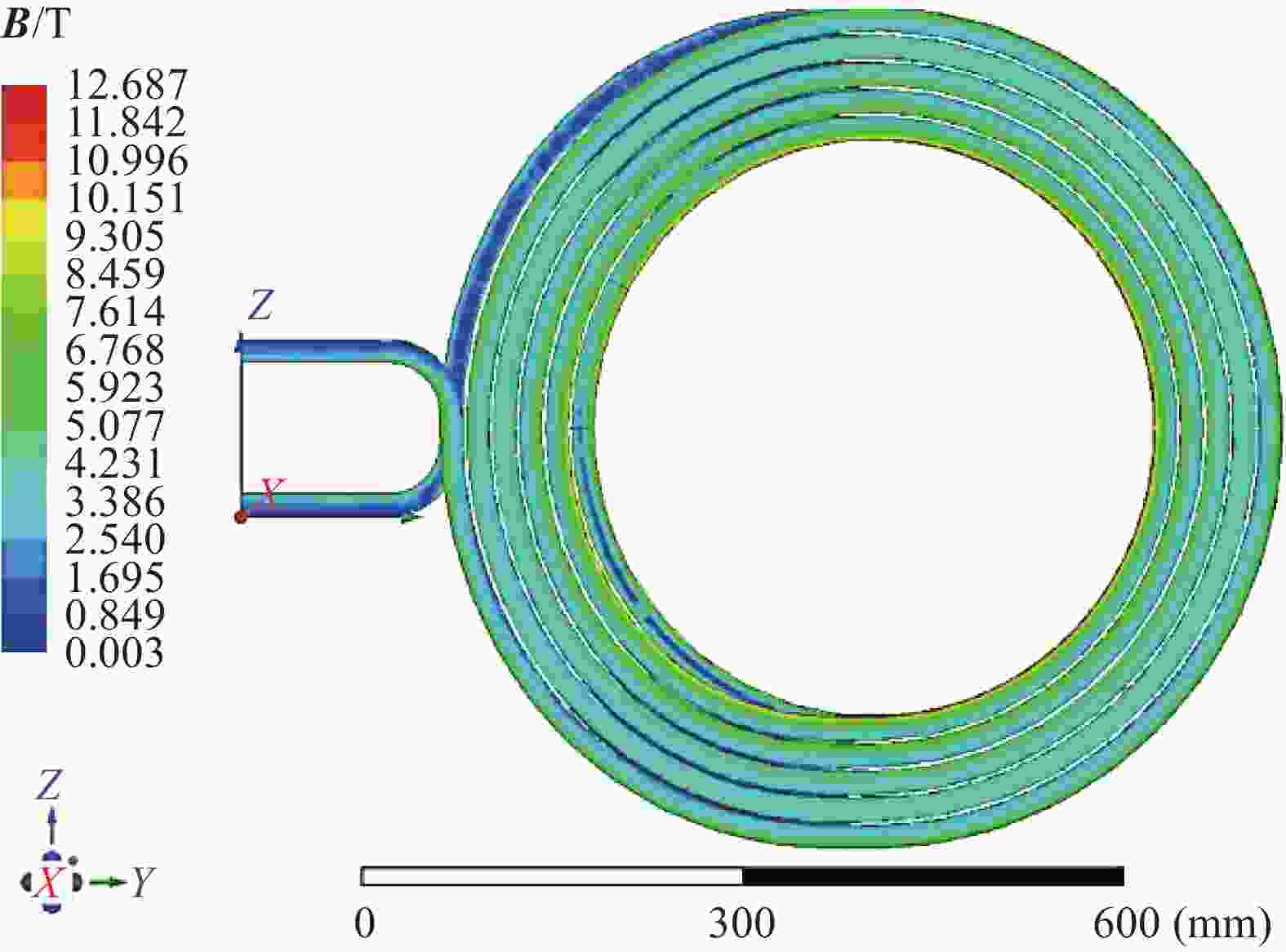
Figure 7. Inner cloud diagram of coil
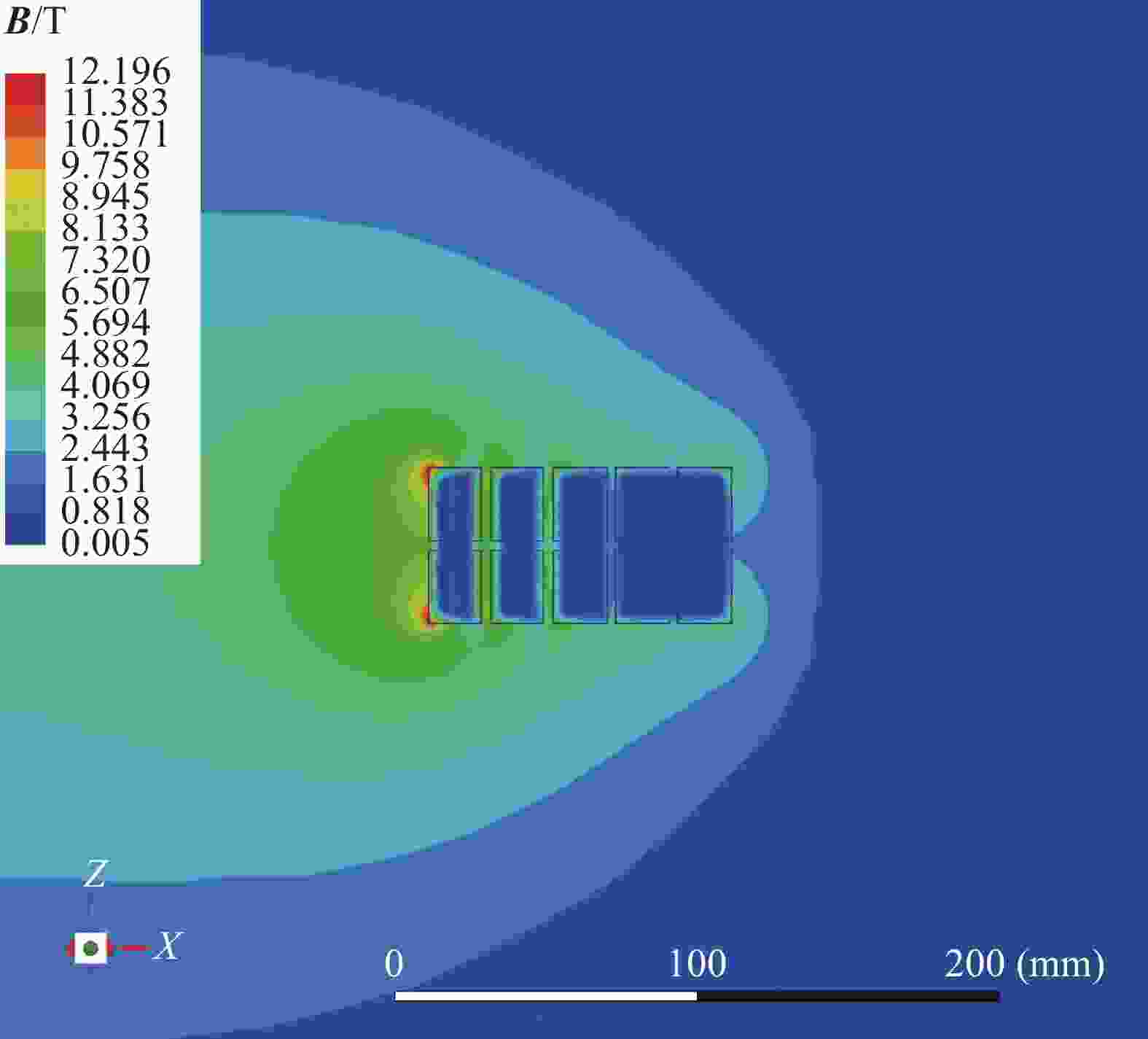
Figure 8. Cloud image of surrounding magnetic field
-
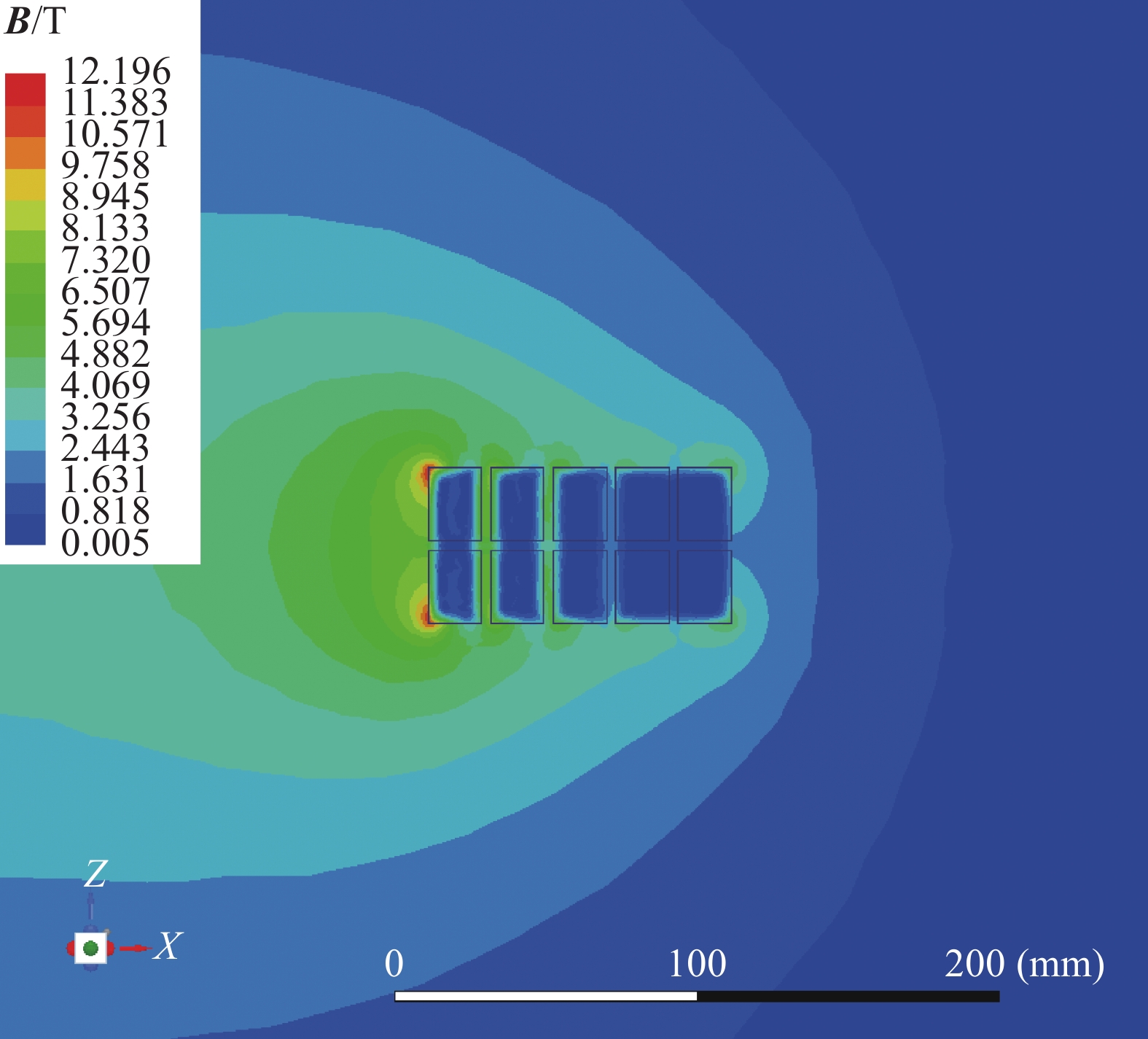
According to Fig. 9, when a pulse current of 120 kA is supplied during the experiment, the copper bar linked below the inductor would deform under the effect of the electromagnetic force, harming the equipment and significantly lowering the auxiliary oscillation zero-crossing circuit's reliability. Therefore, we consider adding a magnetic shielding plate underneath the inductor to reduce the impact of the magnetic field generated by the inductor on the connected copper bar, thus reducing the damage to the equipment.

Figure 9. Field diagram of connecting bar deformation
In the paper, the concept of magnetic field shielding percentage $ S $ is introduced to measure the shielding effect to compare the shielding effect of the magnetic field. The defining equation is shown as Eq. (9):
$$ S=\frac{\boldsymbol{B}_1-\boldsymbol{B}_2}{\boldsymbol{B}_1}\times100\text{%} $$ (9) $ {{\boldsymbol{B}}}_{1} $——the magnetic induction intensity when there is no shielding;
$ {{\boldsymbol{B}}}_{2} $——the magnetic induction intensity with shielding.
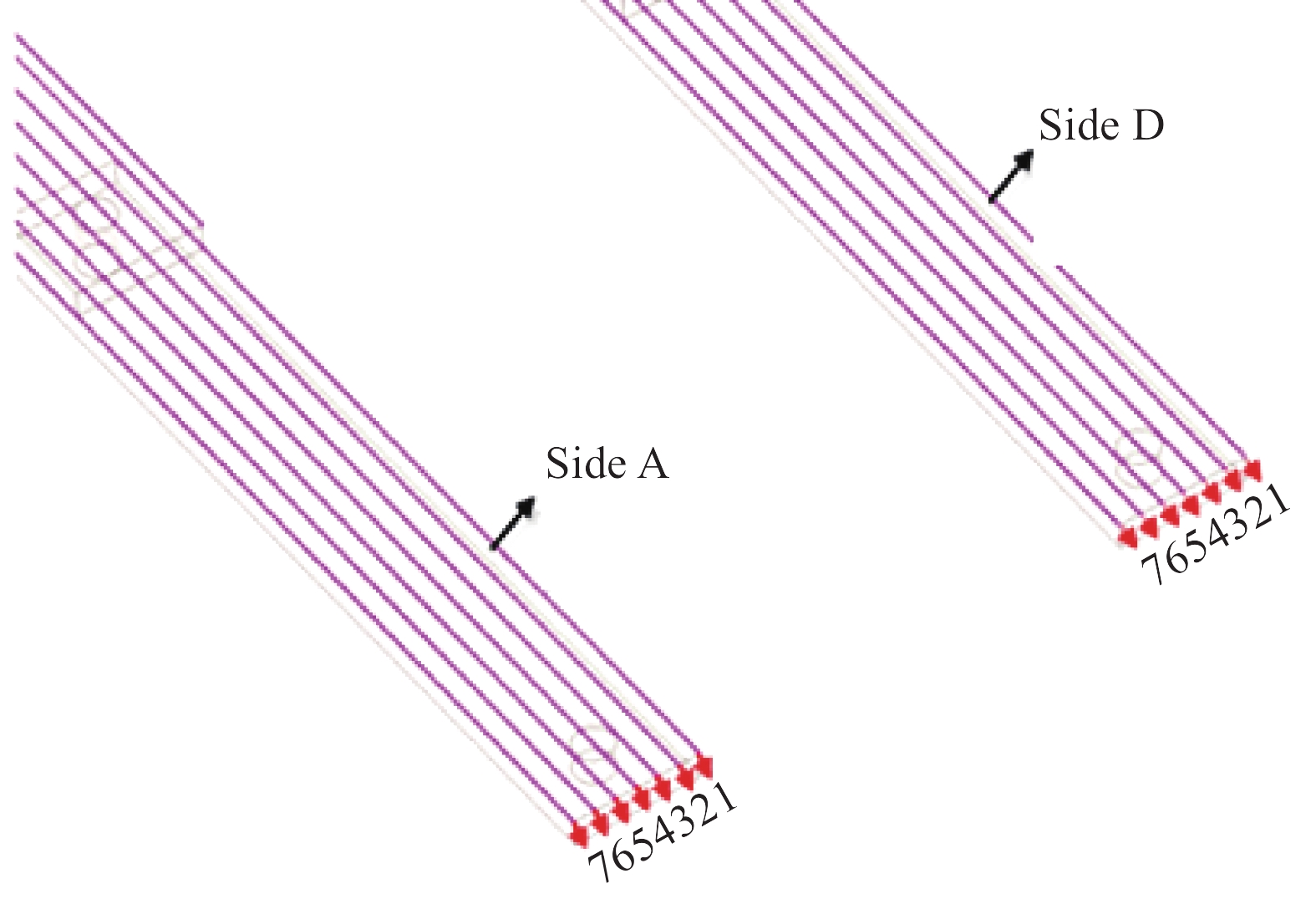
The model diagram of the connecting bar under the pulse inductor, shown in Fig. 10, is established according to the field object. The connecting bar is located under the pulse inductor and consists of six rectangular copper bars connected. To obtain the magnetic induction intensity on each connecting bar, it is numbered as shown in Fig. 11.
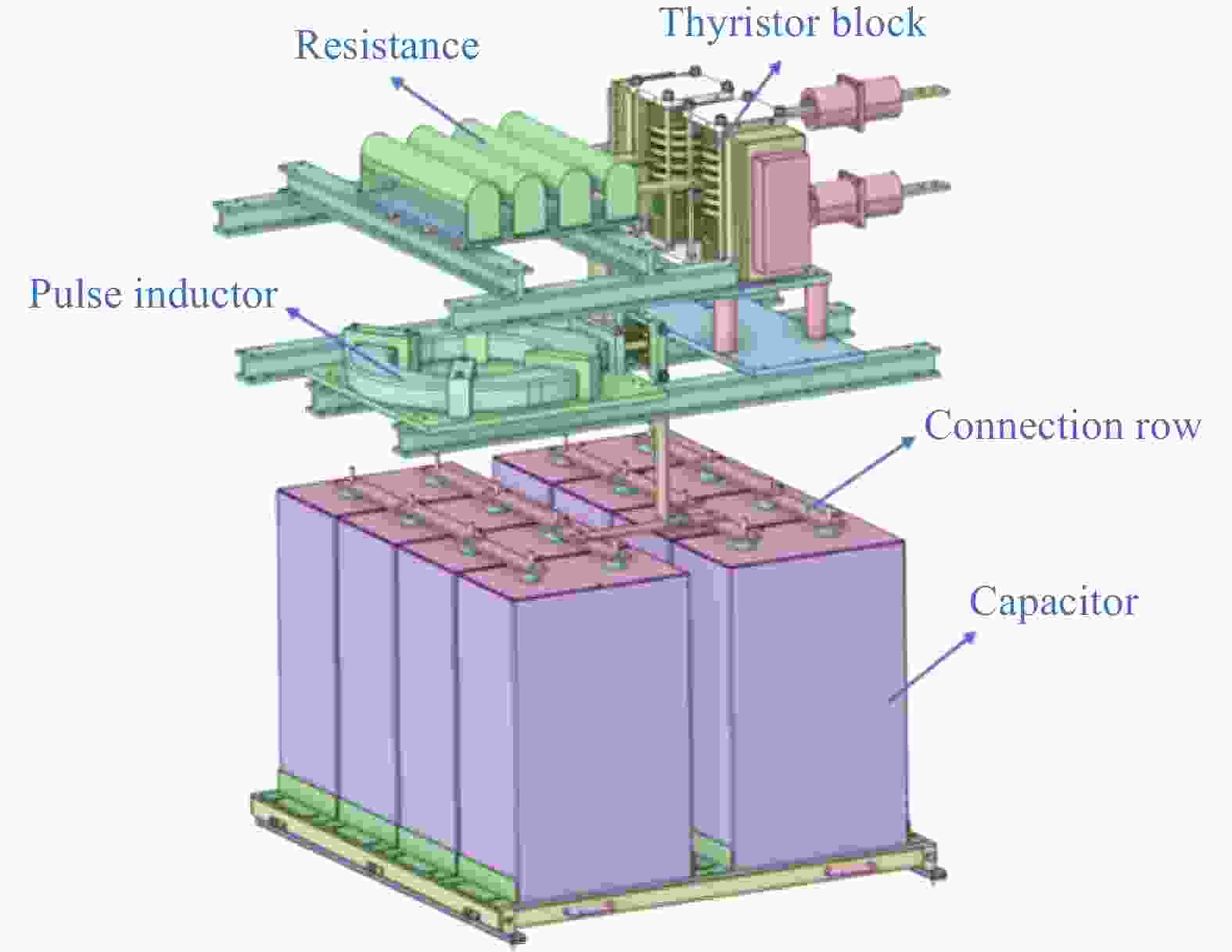
Figure 10. Model diagram of auxiliary oscillation zero-crossing circuit
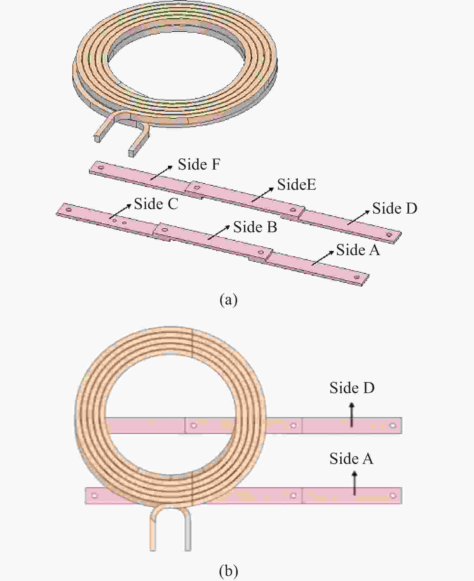
Figure 11. Connecting bar model diagram
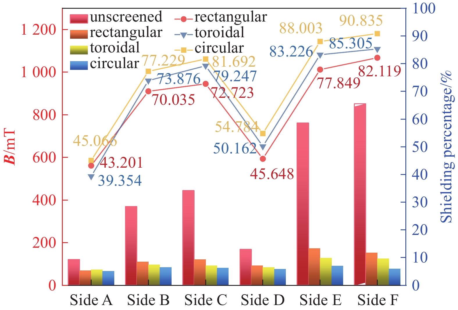
When 120 kA current passes through the pulse inductor, the change in magnetic field intensity of the connecting bar below is observed. Seven lines are taken evenly on each of the two plates, respectively, and 1001 points are taken on each line. The lines are spaced 10 mm apart and oriented from side A to side C (plate 1) and from side D to side F (plate 2). The finite element simulation software Maxwell is used to simulate along the linear direction to get the magnetic induction intensity at different distances along the direction. The connecting bar point diagram is shown in Fig. 12.

Figure 12. Connecting bar point diagram
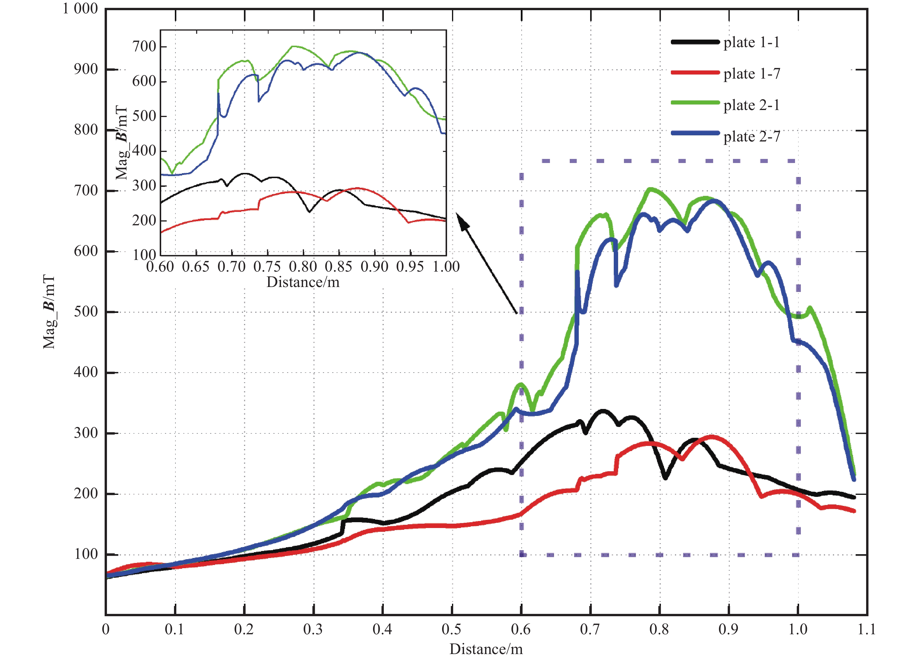
According to Maxwell simulation, the magnetic induction intensity of different points on different straight lines on the connecting bar is obtained, and the data is imported into Origin software to observe the magnitude of magnetic induction intensity at the edge and non-edge of the connecting bar, as well as the magnetic field distribution pattern.
The edge magnetic induction intensity magnitude tends to rise and then fall overall on plate 1 and plate 2 in Fig. 13. In the interval of 0.7 m to 0.9 m, the edge magnetic field intensity on the connecting bar is greater than other points and will be subject to greater electromagnetic force. In Fig. 14, The magnetic induction intensity of the connecting bar is the weakest and the electromagnetic force is the weakest in the non-edge area, between 0.4 m and 0.7 m of the plate. Therefore, it is necessary to shield the connecting bar to reduce the magnetic induction intensity of the connecting bar, reduce the deformation effect caused by the electromagnetic force, and improve the reliability of the system.

Figure 13. Intensity change of magnetic field at the edge of connecting bar

Figure 14. Intensity change of magnetic field at the non-edge of connecting bar
-
First of all, eddy current shielding mainly uses high-conductivity shielding materials to generate eddy currents under time-varying magnetic fields, thus generating a magnetic field opposite to the initial one and offsetting part of the original magnetic field. At the same time, the generated eddy currents will generate losses within the metal shielding body, strengthening the weakening of magnetic field energy, to achieve the shielding effect. Common materials include copper, tin, etc. The flux shunt principle is the use of high magnetic permeability materials, such as iron, nickel steel, and permalloy. The magnetic lines of force are bound within the magnetic material. It will change direction to achieve the shielding effect[20-21].
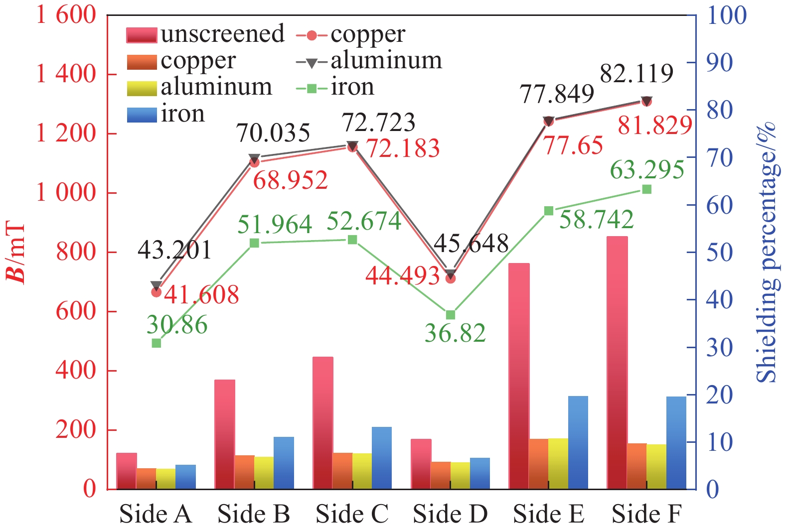
The more common shielding materials in engineering are aluminum, copper, and iron. In this section, aluminum, copper and iron are selected for analysis. The rectangular shield plate shielding is used for simulation. The relative permeability of aluminum and copper is 1, and the relative permeability of iron is taken as 500. The electrical conductivity of aluminum is: 3.82×10⁷ S/m, copper is: 5.80×10⁷ S/m, and iron is: 2.0×10⁷ S/m.
Fig. 15 shows the magnetic induction intensity bar chart and shielding percentage line chart of different shielding materials, and compares the difference of shielding effect of different materials. In the selection of different materials for shielding plates, iron has the worst shielding effect, while aluminum and copper have similar shielding effects. Under economic consideration, aluminum is more economical than copper as the magnetic field shielding material. Therefore, aluminum is the best choice for shielding plate material.
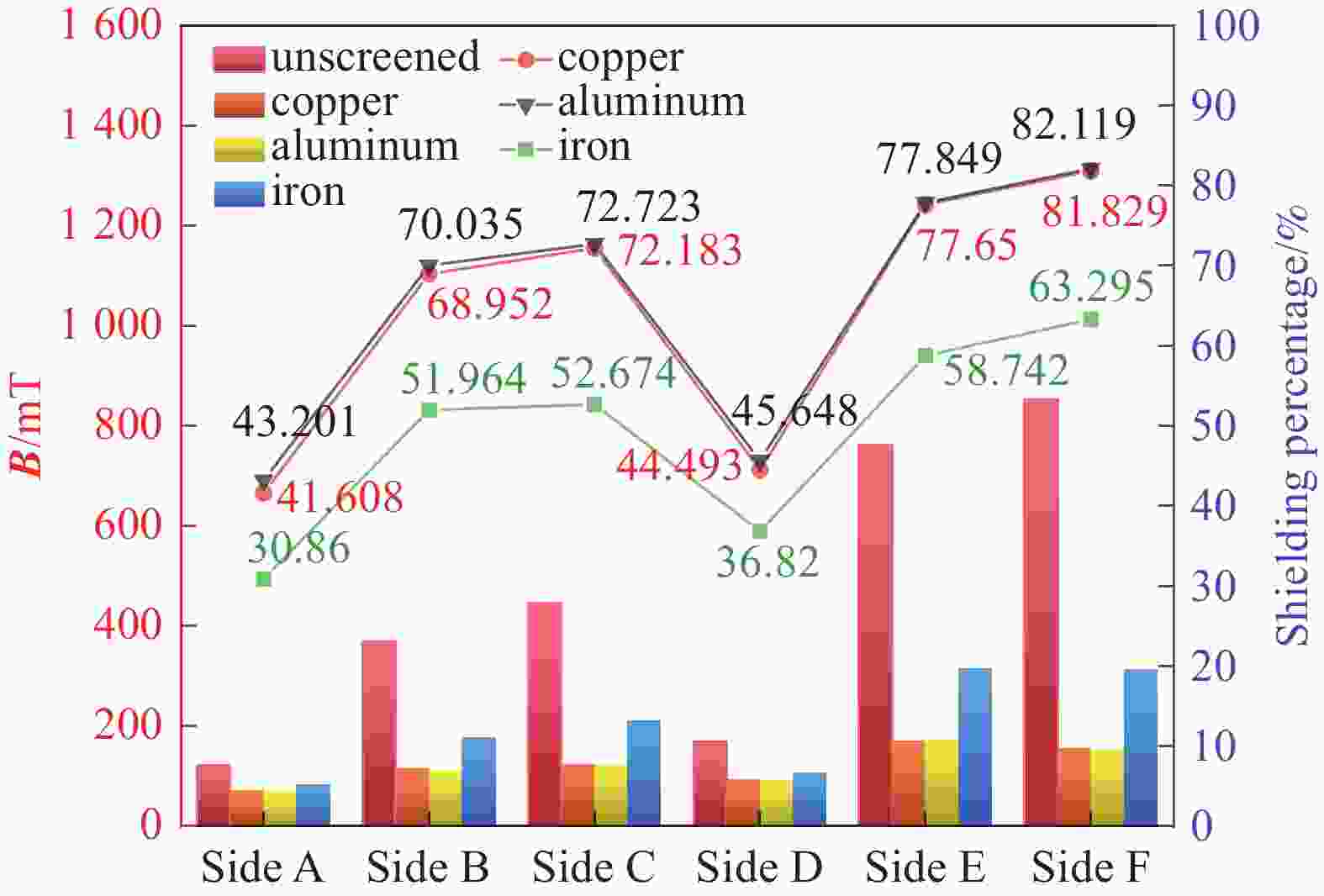
Figure 15. Magnetic induction intensity and shielding percentage of different materials
-
For the alternating magnetic field in the shielded conductor caused by eddy currents, eddy currents in the shielding body produce skin effect. The skinning depth of aluminum at 400 Hz was calculated as 4.07 mm, so the thickness of the plate was taken as 5 mm.
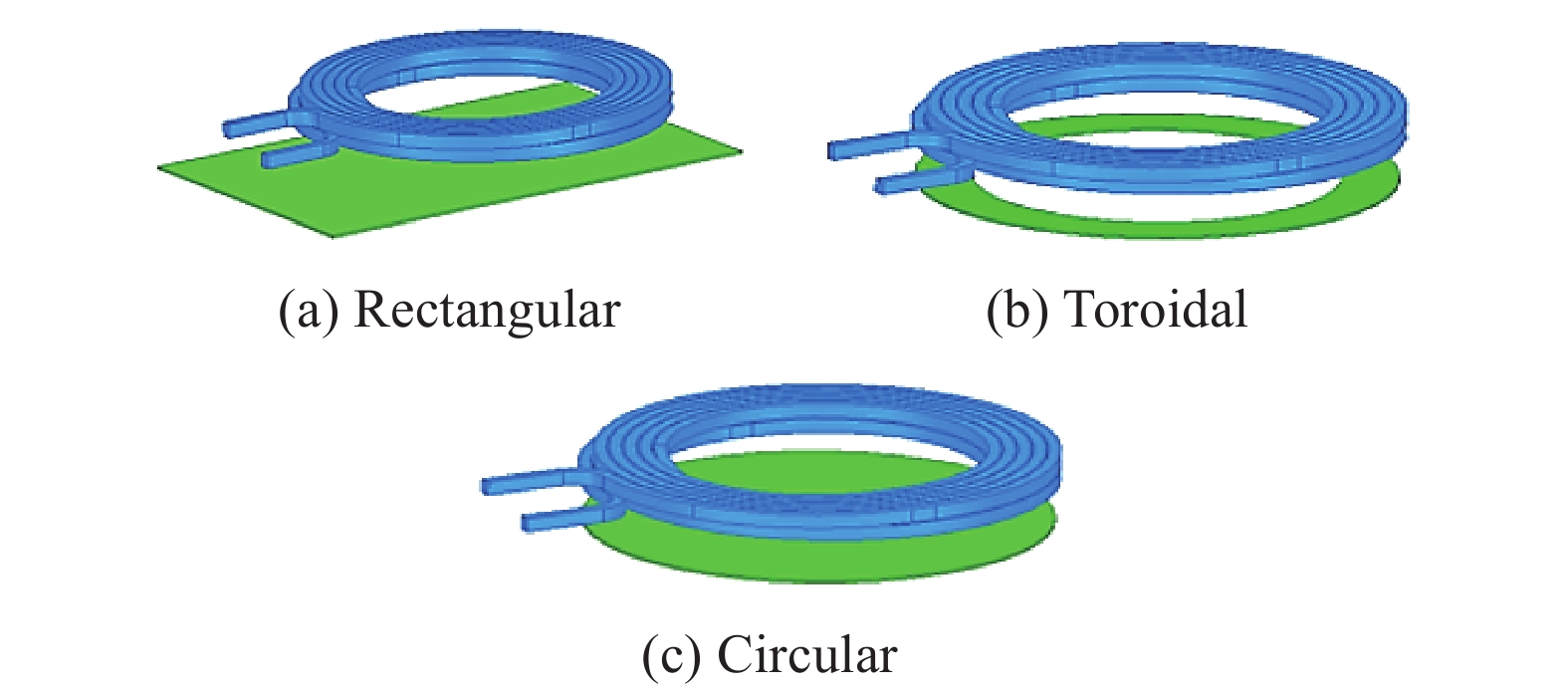
Considering the magnetic field intensity distribution and material economy of the pulsed inductor, three shielding structures are proposed below, as shown in Fig. 16. Using Maxwell software, the magnitude of the magnetic induction intensity applied to the connecting bars under different structures is compared.
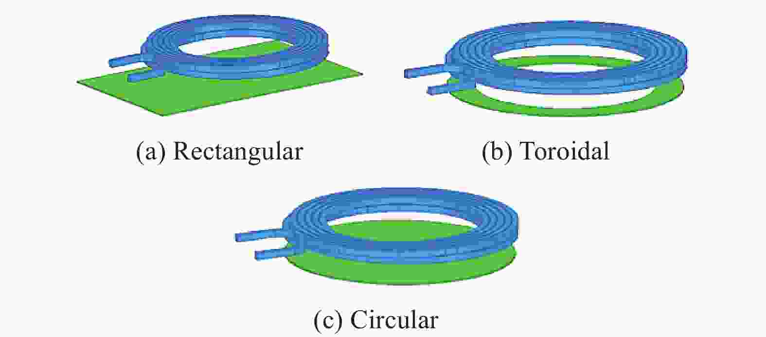
Figure 16. Shield plate construction
Fig. 17 shows the magnetic induction intensity bar chart and shielding percentage line chart under different shielding structures, and compares the influence of different shapes on shielding effectiveness. The comparison shows that there are significant differences in the shielding effects from different shielding structures.
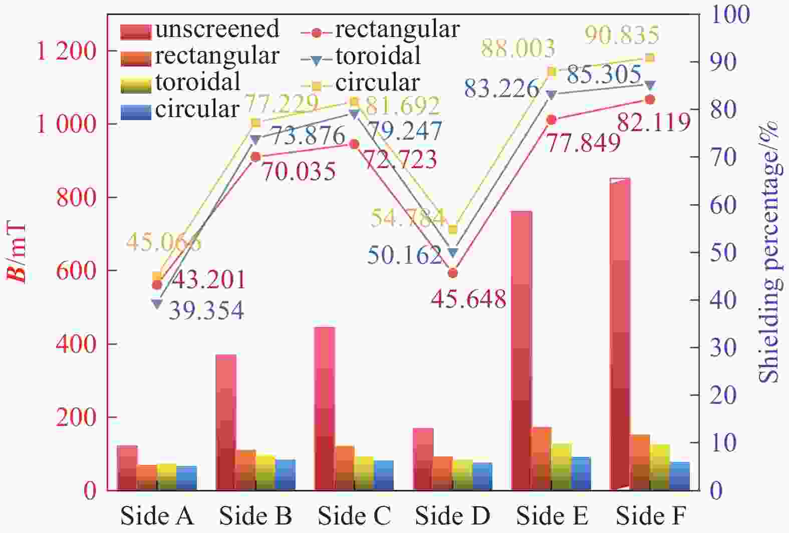
Figure 17. Magnetic induction intensity and shielding percentage of different structures
In Fig. 17, for the circular shielding structure, the magnetic induction intensity of the connecting bar is the smallest. A circular shielding plate is a closed structure that can effectively reduce the penetration of radiation energy, and the surface eddy currents are more uniform and denser, making it easier to form a closed loop. In the toroidal shielding plate, due to the presence of intermittent structures, the eddy current effect may be disturbed or interrupted, leading to instability of the shielding effect or leakage of the magnetic field in some areas. The interference of magnetic leakage and eddy current paths at the edge of the rectangular shielding plate leads to local concentration of the electromagnetic field, thereby reducing the shielding effect. The final choice of a circular shielding plate can effectively reduce the magnetic induction intensity of the connecting bar and improve the reliability of the system.
-
Eddy current loss will result from the alternating magnetic field's impact on the shield plate at high current conditions. It causes energy loss and lowers the effectiveness of the shield. Furthermore, it will cause the shielding equipment's temperature to rise. As a result, the design should aim to reduce eddy current loss as much as possible, and the right shielding structure should be chosen.
$$ {I}_{{\mathrm{t}}}={\int }_{\Omega }\mathit{J}{\mathrm{d}}\Omega ={\int }_{\omega }\dfrac{1}{\mathrm{\mu }}\left(\sigma +\mathrm{j}\omega \epsilon\right)\left(-\mathrm{j}\mathrm{\omega }\mathit{A}-\nabla \mathrm{\varnothing }\right){\mathrm{d}}\omega $$ (10) $$ F=\dfrac{1}{2}\int {{R_{\mathrm{e}}}}\left|\mathit{J}\times \mathit{B}\right|{\mathrm{d}}V $$ (11) Ohmic-loss calculation formula is shown as Eq. (12).
$$ {P}_{{\mathrm{ohmic}}-{\mathrm{loss}}}={\int }_{V}\dfrac{\mathit{J}{\mathit{J}}^{*}}{2\sigma }{\mathrm{d}}V $$ (12) Where:
$ I_\mathrm{t} $ —— total current (A);
$ \mu $ —— permeability of medium (H/M);
$ \sigma $ —— conductivity (S/M);
$ \nabla \mathrm{\varnothing } $ —— gradient of potential (T/M);
$ F $ —— electromagnetic force (N);
Re —— the real part of a complex number;
$ B $ —— magnetic field strength vector (T).
The ohmic loss of the shield plate under various structures is obtained by simulation using a 120 kA current flowing into a three-dimensional time-harmonic field, as shown in Tab. 3.
Shielding structure Ohmic loss/(MW·m-3) Rectangular 32.733 Toroidal 31.761 Circular 11.199 Table 3. Ohmic loss of different shielding structures
Because the model contains multiple conductors, the surface integral of the ohmic-loss density on different shielding bodies is calculated using a field computer, and the eddy current losses of various shielding structures are calculated.
Comparatively, as shown in Tab. 4, the eddy current loss of the toroidal shield plate is the greatest, while that of the rectangular and circular shield plates is comparable. The circular shield is better when taking shape and material into consideration.
Shielding structure Eddy current loss/MW Rectangular 21.668 Toroidal 29.185 Circular 21.957 Table 4. Eddy current loss of different shielding structures
-
According to Maxwell, it was possible to determine the magnetic induction intensity of the connecting bars under various shielding structures. By mapping the results synchronously in the mechanical field, it is possible to see how different shielding structures affect the deformation of the connecting bar.
In a three-dimensional Mechanical, the two ends of the connecting bar are fixed. Considering practical factors, the connecting bar is affected not only by the electromagnetic force transmitted by Maxwell but also by its gravity. In Fig. 18, it is found that the deformation of the connecting bar mainly occurs in the middle part, which is also the place where the electromagnetic force is the greatest.
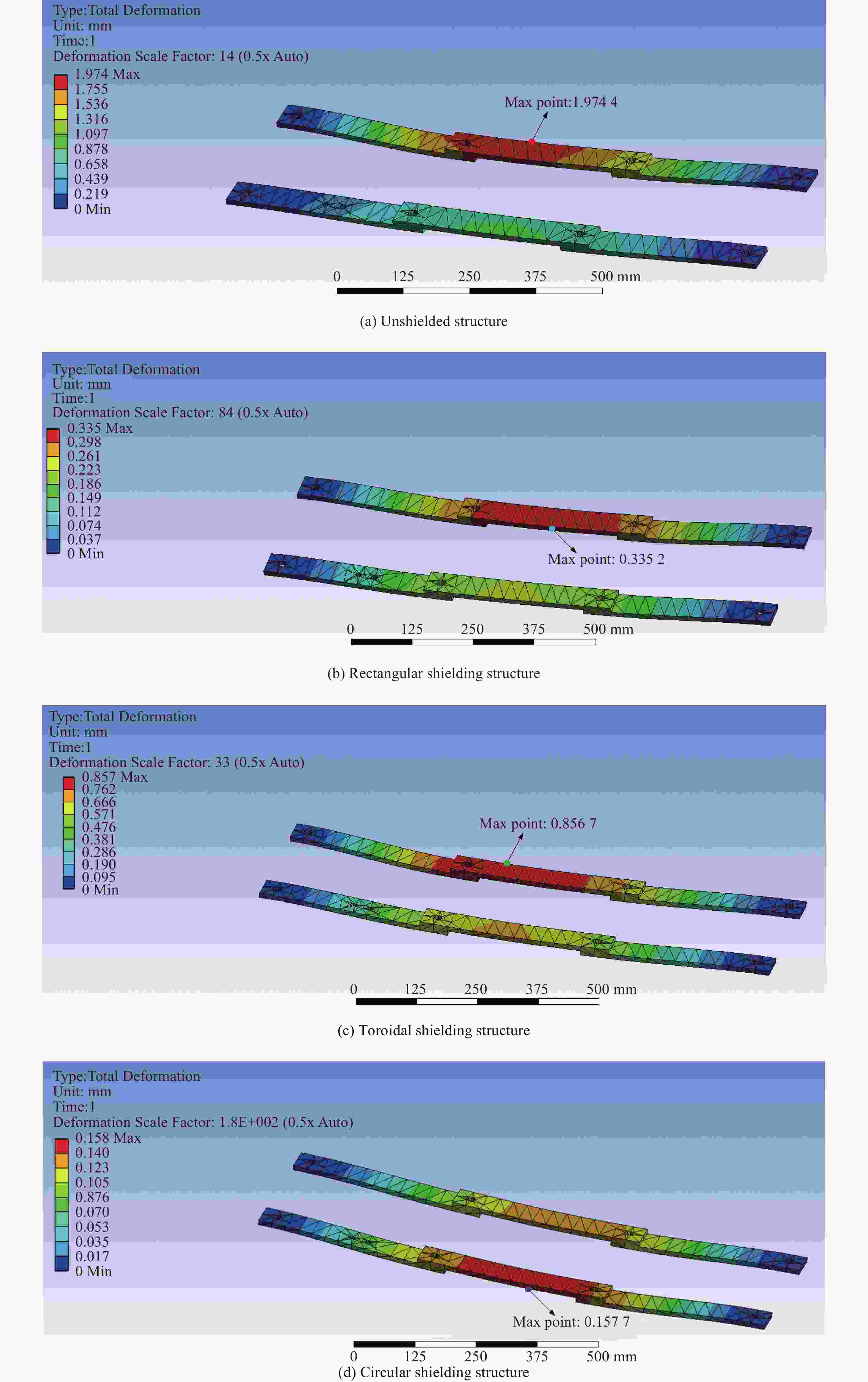
Figure 18. Deformation of connecting bar under different shielding structures
The calculation results are shown in Tab. 5. Calculate the electromagnetic force and equivalent stress on the connecting bar of different shielding structures. The equivalent stress is much lower than the 250 MPa yield strength of the connecting bar, and the safety margin is sufficient. When the pulse inductor is not shielded, the maximum deformation of the connecting bar reaches 1.974 mm. The connecting bar variable is significantly lessened by masking. Among them, the circular shield structure has the best effect, with the maximum shape variable of 0.158 mm and the average shape variable of 0.079 mm. This successfully lessens the impact of the electromagnetic force produced by the pulsed inductor on the surrounding machinery.
Shielding structure Connecting bar
electromagnetic force/NEquivalent stress/
MPaMaximum deformation/
mmAverage deformation/
mmUnshielded 809.630 - 1.974 0.712 Rectangular 264.320 13.6 0.335 0.157 Toroidal 467.810 30.5 0.857 0.420 Circular 72.185 10.3 0.158 0.079 #Note: The yield strength of copper is 250 MPa, and the ultimate tensile strength is 343 MPa. Table 5. Connecting bar deformations under different shielding structures
-
In this article, when the shielding plate material is aluminum, the pulse inductor has the best optimization effect on the electromagnetic field distribution of the connecting bar. When considering the shielding plate structure, the shielding effect of circular shielding plates is the most ideal. In summary, the use of circular aluminum shielding plates can effectively reduce the magnetic induction intensity and electromagnetic force of the connecting bar, and improve the overall reliability of the QPS. However, the simulation in this article only analyzes and calculates the influence of shielding plate materials and structures on the electromagnetic distribution of pulse inductors. Therefore, this conclusion will be verified through experiments in the next step, and other factors affecting the shielding effect will be considered.
Optimization of Electromagnetic Field Distribution of 120 kA Pulse Inductor in Oscillation Discharge Circuit
doi: 10.16516/j.ceec.2024.3.03
- Received Date: 2024-01-22
- Accepted Date: 2024-03-18
- Rev Recd Date: 2024-03-16
- Available Online: 2024-04-22
- Publish Date: 2024-05-10
-
Key words:
- pulse inductor /
- shielding plate /
- shielding percentage /
- auxiliary oscillation /
- quench protection system
Abstract:
| Citation: | LI Zhenhan, LI Hua, BAO Xiaohua, et al. Optimization of electromagnetic field distribution of 120 kA pulse inductor in oscillation discharge circuit [J]. Southern energy construction, 2024, 11(3): 23-35. DOI: 10.16516/j.ceec.2024.3.03 doi: 10.16516/j.ceec.2024.3.03

|

 DownLoad: